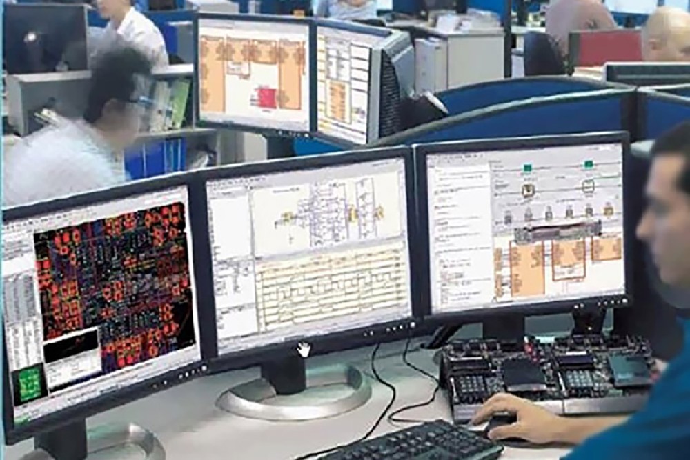
A professional design team over 10 years of design work experience
A complete solution from schematic, layout, wiring to photo file generation
Having strong production and design capabilities, and rich experience in PCBA product development
A comprehensive PCB circuit board design process and profound practical experience in PCB design
The parameters of PCB design are not only suitable for the research and development stage, but also fully consider the mass production characteristics
Design Capability
| Minimum Line Width | 2.5MIL |
| Minimum Spacing | 2.5MIL |
| Minimum Through-hole | 6MIL (4MIL laser hole) |
| The Highest Number of Layer | 32 |
| Minimum BGA Spacing | 0.4MM |
| Maximum BGA PIN Count | 2500PINs |
| Highest speed signal | 12G differential signal |
| The highest number of HDI Layers | 18 |
| DHI Highest Layers | 10 Any Order HDI |
Technologies Employed
1. Strong theoretical and practical skills in electromagnetic fields, as well as strong technical background and support.
2. Proficient EDA usage skills.
3. Signal integrity simulation analysis (impedance control, reflection, crosstalk, timing)+years of experience accumulation.
4. Power ground integrity analysis.
5. Board EMC design, decoupling, with rich experience in single board EMC/EMI design
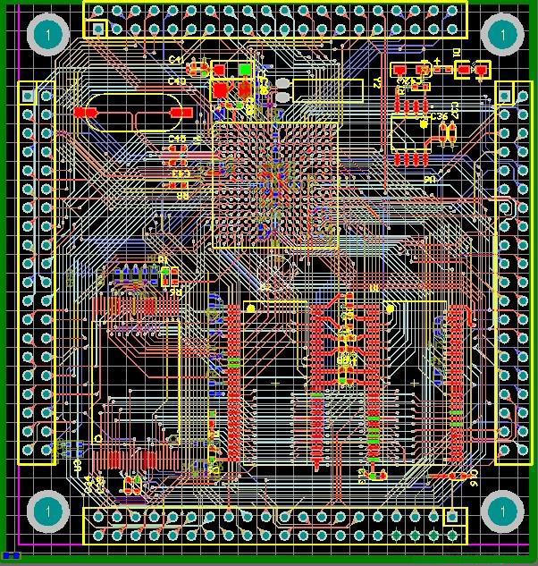
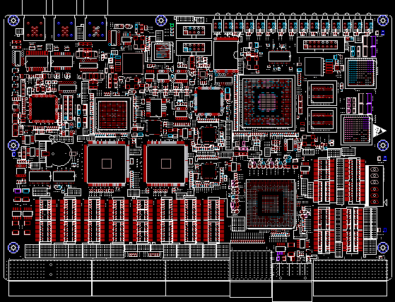
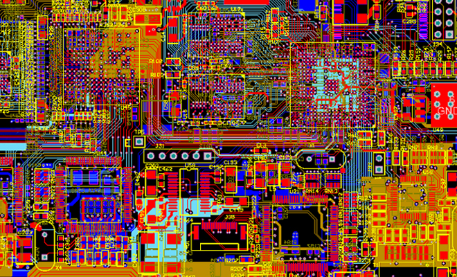
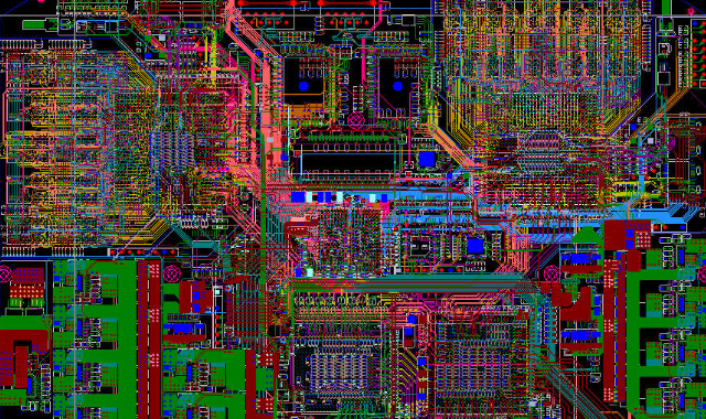
Cases