Wanlong is PCB board manufacturer with a monthly production capacity of 100000 square meters
PCB board making processes include lead-free tin deposition, tin spraying, gold deposition, electroplating, chemical silver, OSP, etc
The substrates used for PCB production include A-grade materials from Shengyi, KB, and Jinan International FR4. Suppliers of substrates for high-frequency and special boards include Rogers, Taconic, and others
Wanlong Manufacturing provides fast service, quality assurance, fast delivery time, and on-time delivery.
PCB Production Capacibility
| Maximum Layers | 32 |
| Mass Production Capacibility | 16 |
| Sample Production Capacibility | 32 |
| Minimum Dimension | 60x60mm |
| Maximum Dimension | 550x560mm |
| Thickness of board | 0.4~5mm |
| Size of Components | 0.201~150mm |
| Maximum Height of Components | 25mm |
| Minimum Pin Distances | 0.2mm |
| Minimum Line Width and Line Spacing | 3/3mil 4/4mil(Finished copper thickness1 OZ) 5/5mil(Finished copper thickness1.5 OZ) 6/6mi |
| Minimum aperture (machine drilling) | 0.2mm |
| Aperture tolerance (machine drilling) | ±0.07mm |
| Aperture tolerance (laser drill) | ±0.01mm |
| Through hole unilateral welding ring | 3mil |
| Effective Line Bridge | 6mil |
| Finished product outer layer copper thickness | 35~140um |
| Finished inner layer copper thickness | 17~35um |
| Resistance welding type | Photosensitive ink |
| Minimum character width | ≧0.15mm |
| Minimum character height | ≧1mm |
| Character aspect ratio | 1:05 |
| Surface treatment | Carbon oil, tin spraying, lead-free tin spraying, gold sinking, silver sinking, OSP, gold finger, selective gold sinking, electroplated gold, HAL |
| Minimum slot knife | 0.65mm |
| Distance between wiring and appearance | The distance between the routing layer and the outer line of the board for shipment of gong boards shall not be less than 0.25mm; V-cut panel shipment, the distance between the wiring and the V-cut centerline cannot be less than 0.4mm |
| Minimum half hole diameter for half hole process | 0.6mm |
| Assembly: No gap assembly gap | 0mm gap splicing |
| Assembly: With gaps in the assembly process | 1.6mm |
| Peeling strength | >2.0N/cm |
| Flame retardancy | 94V-0 |
| Impedance control tolerance | ±10% |
| Pads manufacturer's copper laying method | Hatch copper laying method |
| Drawing slots in Pads software | Using Drill Drawing Layer |
| Window layer in Protel/dxp software | Solder layer |
| Special craftsmanship | Resin dense holes, holes in the plate, mixed pressure plate, PTFE, blind buried holes, and bound ICs (special processes require process review before being taken offline) |
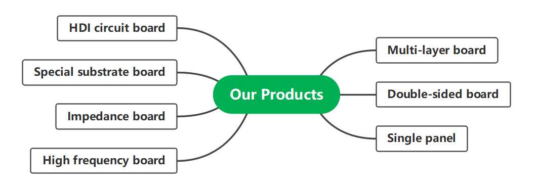
| Board type | FR-4、 High frequency boards, Rogers, and FR4 boards use Jiantao A-grade materials on both sides, and multi-layer boards use raw materials |
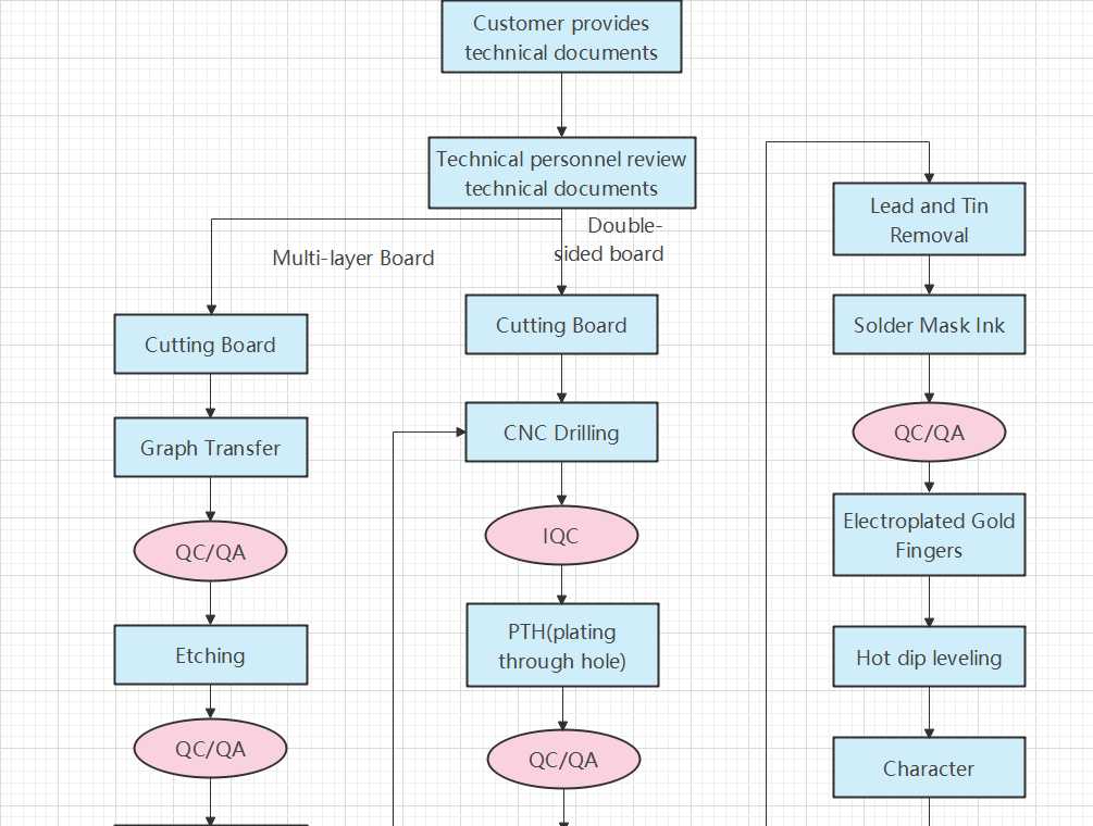
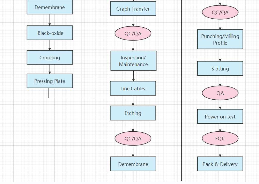
PCB Production Process